From American Affairs Journal, Volume VIII, Number 1, Spring 2024:
Since I last wrote in detail on the topic of China’s domestic semiconductor industry in early 2021,1
the landscape has changed considerably. The Biden administration has
continued to impose export control restrictions on Chinese firms, and
the October 7, 2022, package of controls targeted not only advanced
semiconductors (such as GPUs used for running artificial intelligence
and machine learning workloads) but also expanded significantly on
controls over semiconductor manufacturing equipment (SME).2
One goal of the U.S. controls is to prevent Chinese firms from moving
into nonplanar technology processes, such as FinFET and eventually Gate
All Around (GAA). The new restrictions included novel end-use controls
and controls on U.S. persons, posing major new challenges for China’s
domestic semiconductor industry development going forward.3
Updates to the October 2022 controls released on October 17, 2023,
followed this approach, and introduced more challenges for China’s
semiconductor industry. To an extent not apparent in 2021, the long-term
ability of Chinese firms to source advanced semiconductors is now much
more closely tied to the speed of development of China’s domestic
toolmaking and manufacturing capabilities, given the substantial
increase in the number of Chinese design firms now unable to use foreign
foundries.
U.S. controls are impacting only cutting-edge capabilities, so
Chinese firms will continue to expand capacity at mature nodes where the
bulk of the domestic demand remains. At more advanced nodes below 28
nanometers, leading Chinese firms continue to have access to some
advanced Western tools, particularly deep ultraviolet (DUV) immersion
lithography systems, that they will continue to use for as long as
possible to stretch logic production at more advanced nodes,
particularly down to 7 and even 5 nanometers. Nevertheless, it is
important to note that using DUV tools for advanced node production is
complex, because using techniques like multi-patterning also requires
advanced capabilities in other key tools such as deposition and etch.
For advanced node production, tight coupling of key processing tools is
required, and the issue is not just about lithography tools, as media
and other commentary on China’s semiconductor industry typically
emphasizes. Materials such as photoresists are also critical to the
process of extending DUV capabilities to fine feature lengths at 7
nanometers and below.
Even though U.S. controls have so far focused on advanced
manufacturing capabilities, Beijing and Chinese companies are also
worried about future controls, and will prioritize tool and material
production lines free of Western inputs to reduce long-term risks.
Hence, even if they can still acquire Western tools, virtually all
leading Chinese foundries and memory companies are working methodically
with domestic toolmakers to develop and validate equipment to
eventually establish production processes largely free of Western
equipment. This will be a multistage, multiyear process, starting with
40 nanometers and proceeding quickly, likely this year, to 28
nanometers, and then 14, 12/10, and eventually 7 nanometers. Continued
access to Western tools such as DUV—coupled with some foreign and increasingly domestic etch and deposition tools—can
provide a bridge to an all-domestic future for Chinese semiconductor
manufacturing. From an overall semiconductor industry viewpoint, what is
happening in China will fundamentally change the industry over the next
decade.4
In addition, officials in Beijing are developing new approaches to
public-private collaboration to push innovation on key technologies,
such as advanced lithography. Beijing, working closely with the private
sector, is looking to overcome bottlenecks by easing the transfer of
advanced state-backed R&D to designated private sector companies, by
pushing companies to work together on critical technologies, and by
pursuing approaches that have been successful in other sectors. These
approaches include having a large state-owned firm play a leading role
in the sector while funding and facilitating multiple teams to tackle
tough problems, as was done for exascale computing.5
Many other pieces of the semiconductor manufacturing industry are
also targets of renewed efforts to build domestic Chinese alternatives,
such as design tools, advanced materials, advanced packaging techniques,
and systems engineering approaches designed to improve performance via a
systems-led approach, rather than relying solely on process-node
improvements. All of these approaches will be important for China’s
domestic capabilities going forward, particularly packaging, including
chiplet design and 2.5 and 3-d back-end
packaging approaches, that will feature in system engineering efforts to
improve performance levels and bridge to new, domestic-only production
processes.
None of this will be easy or guaranteed to succeed, in the sense of
producing end products comparable to those of the mainstream global
semiconductor manufacturing process. These efforts will also produce
winners and losers, with Western tool makers perhaps the biggest
victims as they are gradually frozen out of what had been a huge,
growing, and lucrative market that they dominated before October 7,
2022. Still, parts of China’s semiconductor sector will retain greater
linkage with global developments and supply chains than others, and the
overall situation will continue to be complex and evolving.
Sweeping Controls on Tools Target China’s
Domestic Manufacturing Industry
When Secretary of State Antony Blinken put technology competition at
the center of U.S.-China relations and competition in May 2022,6
few likely realized the extent of what was to follow later that year.
In the fall of 2022, the Biden administration, for the first time, had
senior officials articulate the U.S. strategic policy toward
semiconductors and China, as expressed by National Security Advisor Jake
Sullivan and other senior officials, such as Undersecretary of Commerce
Alan Estevez. The “Sullivan Doctrine,” as articulated in late 2022,
includes several parts, starting with Sullivan’s assertion that the
United States intends to maintain an absolute lead over China in key
sectors, rather than a sliding scale. He also indicated that the United
States was implementing a “small yard, high fence” approach toward China
and advanced technologies,7
and further asserted that technologies such as advanced computing
(semiconductors as well as AI, machine learning, and high-performance
computing), biotechnology, and green/clean technology were “truly force
multipliers” throughout the tech ecosystem. The Sullivan Doctrine’s
bottom line: leadership in each of these areas is a “national security
imperative.”8
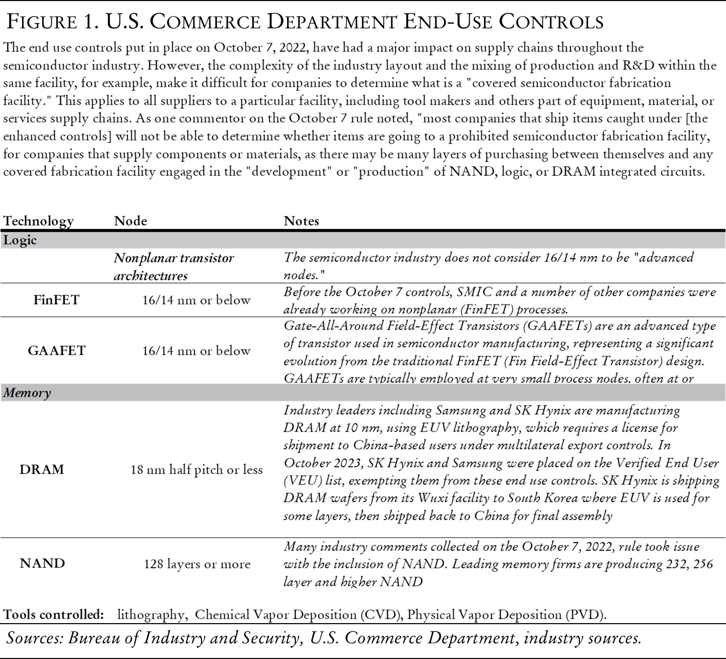
The most complex and controversial portions of the October 7, 2022, rules released by the Commerce Department9
were the end-use controls on semiconductor manufacturing tools, and on
U.S. persons. The SME controls call for licensing of equipment and U.S.
persons for manufacturing of logic semiconductors at 16/14 nanometers,
3-d NAND memory at 128 layers, and DRAM
at 18 nanometers half pitch. The result of these controls, initially
dropped unilaterally, without agreement from other key countries whose
companies occupy critical portions of the SME supply chain—namely Japan and the Netherlands—was
that leading U.S. toolmakers, such as Applied Materials, KLA Tencor,
and Lam Research were forced to pull all their U.S. personnel from
facilities in China, particularly at foundry leader SMIC, NAND memory
giant YMTC, and DRAM major CXMT. In addition, the package of
restrictions also imposed controls on inputs to Chinese domestic
semiconductor equipment makers, in a bid to keep them from replacing
foreign equipment leaders. Almost overnight, the entire Chinese
domestic manufacturing and toolmaking equipment sector was thrown into a
completely new era.
The October 2023 update10
to these rules has only added to the challenges Chinese semiconductor
firms face. The new controls tightened thresholds around specific
parameters used for some much older ASML DUV lithography tools, again
moving the goalposts. The 2023 package also raised thresholds for
performance of advanced GPUs that could be sold to Chinese end users,
capturing a number of GPUs that global leader Nvidia had redesigned for
the China market to comply with restrictions in the 2022 package.
For China’s domestic industry, the most important impact of the
controls was to massively incentivize designing U.S. technology out of
the semiconductor space, by both Chinese domestic and foreign firms.
Prior to this, Chinese technology firms acquired and used the most
advanced equipment and services available, like their peers and
competitors globally. Many observers still erroneously claim that
China’s Made in China 2025 strategy (announced in 2015) was a signal
that Beijing wanted to go it alone in key sectors. A side-study linked
to Made in China 2025 listed wildly unrealistic goals for domestic
proportions of different types of semiconductor production, but this
hardly represented a concerted government policy, and Chinese
semiconductor companies largely ignored it. That changed in 2023. Senior
Chinese semiconductor industry experts stress that domestic industry
players would prefer to use the best available tools, but are now under
increasing pressure to favor domestic firms and develop alternative
supply chains.11
Chinese Reactions to New U.S. Controls
As the events of October 2022 began to play out in China and around
the world, and Chinese industrial planners, company executives, and
foreign partners assessed the damage, several critical issues emerged
that will determine the future direction of China’s semiconductor
industry.
First, the unilateral nature of the controls has necessitated a long
and painful dialogue between the U.S. government and the governments of
the Netherlands and Japan around how to align on the controls. This
so-called trilateral group had been discussing controls on SME for
nearly two years, but both Japan and the Netherlands preferred setting
any end‑use controls at more advanced nodes, at 10 nanometers or below.
When the U.S. side set the end-use controls at 16/14 nanometers, the
trilateral talks broke down. U.S. officials were apparently under
pressure from the Department of Defense, which had grown concerned by
reports over the summer of 2022 that SMIC had been able to produce
semiconductors with some layers at 7 nanometers—using
existing deep ultraviolet (DUV) lithography gear and other foreign and
domestic tools such as etch and deposition. This was one of many
instances in which the U.S. semiconductor industry felt that the Biden
administration was “moving the goalposts” around the parameters for
controls on technology for Chinese end users.12
The U.S. government badly underestimated the political and industry
pushback on the unilateral controls. All talk of a “trilateral
agreement” was quickly dropped, and privately, U.S. officials began
speaking more about “leveling the playing field” and “burden sharing.”13
Neither the Japanese nor Dutch governments wanted to be part of an
agreement visibly directed at containing China’s technology ambitions,
and both governments have received major pushback from their leading
semiconductor firms. At the same time, neither the Japanese, the Dutch,
nor the toolmaking industry were expecting memory to be included in the
controls....
....MUCH MORE